 购物车0
购物车0
Please consider this device
dsPIC33F General Purpose Digital Signal Controller with seamless migration options to PIC24F,MCUs and dsPIC30F DSC
Operating Range:DC – 40 MIPS (40 MIPS @ 3.0-3.6V, -40°C to +85°C)
Industrial temperature range (-40°C to +85°C)High-Performance DSC CPU:
Modified Harvard architecture
C compiler optimized instruction set
16-bit wide data path
24-bit wide instructions
Linear program memory addressing up to 4M instruction words
Linear data memory addressing up to 64 Kbytes
83 base instructions: mostly 1 word/1 cycle
Sixteen 16-bit General Purpose Registers
Two 40-bit accumulators:- With rounding and saturation options
Flexible and powerful addressing modes:- Indirect, Modulo and Bit-Reversed
Software stack
16 x 16 fractional/integer multiply operations
32/16 and 16/16 divide operations
Single-cycle multiply and accumulate:- Accumulator write back for DSP operations- Dual data fetch
Up to ±16-bit shifts for up to 40-bit dataDirect Memory Access (DMA):
8-channel hardware DMA:
2 Kbytes dual ported DMA buffer area (DMA RAM) to store data transferred via DMA:- Allows data transfer between RAM and a peripheral while CPU is executing code (no cycle stealing)
Most peripherals support DMAInterrupt Controller:
5-cycle latency
118 interrupt vectors
Up to 67 available interrupt sources
Up to 5 external interrupts
7 programmable priority levels
5 processor exceptionsDigital I/O:
Wake-up/Interrupt-on-Change on up to 24 pins
Output pins can drive from 3.0V to 3.6V
All digital input pins are 5V tolerant
4 mA sink on all I/O pinsSystem Management:
Flexible clock options:- External, crystal, resonator, internal RC- Fully integrated PLL- Extremely low jitter PLL
Power-up Timer
Oscillator Start-up Timer/Stabilizer
Watchdog Timer with its own RC oscillator
Fail-Safe Clock Monitor
Reset by multiple sourcesPower Management:
On-chip 2.5V voltage regulator
Switch between clock sources in real time
Idle, Sleep and Doze modes with fast wake-upTimers/Capture/Compare/PWM:
Timer/Counters, up to nine 16-bit timers:- Can pair up to make four 32-bit timers- 1 timer runs as Real-Time Clock with external 32.768 kHz oscillator- Programmable prescaler
Input Capture (up to 8 channels):- Capture on up, down or both edges- 16-bit capture input functions- 4-deep FIFO on each capture
Output Compare (up to 8 channels):- Single or Dual 16-Bit Compare mode- 16-bit Glitchless PWM modeCommunication Modules:
3-wire SPI (up to 2 modules):- Framing supports I/O interface to simple codecs- Supports 8-bit and 16-bit data- Supports all serial clock formats and sampling modes
I2C™ (up to 2 modules):- Full Multi-Master Slave mode support- 7-bit and 10-bit addressing- Bus collision detection and arbitration- Integrated signal conditioning- Slave address masking
UART (up to 2 modules):- Interrupt on address bit detect- Interrupt on UART error- Wake-up on Start bit from Sleep mode- 4-character TX and RX FIFO buffers- LIN bus support- IrDA® encoding and decoding in hardware- High-Speed Baud mode- Hardware Flow Control with CTS and RTS
Data Converter Interface (DCI) module:- Codec interface- Supports I2S and AC’97 protocols- Up to 16-bit data words, up to 16 words per frame- 4-word deep TX and RX buffers
Enhanced CAN (ECAN™ module) 2.0B active (up to 2 modules):- Up to 8 transmit and up to 32 receive buffers- 16 receive filters and 3 masks- Loopback, Listen Only and Listen All Messages modes for diagnostics and bus monitoring- Wake-up on CAN message- Automatic processing of Remote Transmission Requests- FIFO mode using DMA- DeviceNet™ addressing supportAnalog-to-Digital Converters (ADCs):
Up to two ADC modules in a device
10-bit, 1.1 Msps or 12-bit, 500 Ksps conversion:- 2, 4 or 8 simultaneous samples- Up to 32 input channels with auto-scanning- Conversion start can be manual or synchronized with 1 of 4 trigger sources- Conversion possible in Sleep mode- ±2 LSb max integral nonlinearity- ±1 LSb max differential nonlinearityCMOS Flash Technology:
Low-power, high-speed Flash technology
Fully static design
3.3V (±10%) operating voltage
Industrial temperature
Low-power consumption

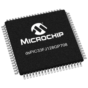
DSPIC33FJ128GP708 封装图
| 型号 | 制造商 | 描述 | 购买 |
|---|---|---|---|
| DSPIC33FJ128GP708-I/PT | SSI | SENSOR 200PSI 3/8-24UNF .5-4.5V | 立即购买 |
图1给出了dsPIC33CH系列MCU主核与从核共享内部合外部振荡器源的框图,也就是说主核和从核共享时钟源,但是振荡器模块是完全独立的。
Microchip公司的dsPIC33FJ06GS101 / X02和dsPIC33FJ16GSX02 / X04包括了DSP功能和高性能16位MCU架构,在3.0-3.6V时可达40MIPS,大约有35个可编数字I / O,闪存容量16KB,集成了dsPIC33F系列产品的主要特性,其中图是集成了高速PWM模块,中断控制器,...
...备的保护电源。本文介绍了UPS参考设计的主要指标,采用dsPIC33FJ16GS504的离线UPS机箱图,电路图,材料清单和PCB元件布局图。
Microchip Technology dsPIC33CK64MC105 Curiosity Nano评估套件是用于评估dsPIC33CK64MC105微控制器的硬件平台。Microchip
本文介绍了dsPIC33FJ系列主要特性,方框图和CPU 核方框图,DSP 引擎方框图,数字PFC框图以及多种应用框图。此外还介绍了相移全桥(PSFB) 1/4砖形DC-DC转换器参考设计主要特性和指
本视频介绍了Microchip脉搏血氧仪演示板,通过Microchip dsPIC33FJ128GP802高性能数字信号控制器(DSC)来实现。该参考演示板可帮助设计人员开发带有用户界面的低成本手持式或可穿戴式脉搏血氧仪,实现同时测量心率和血氧饱和度。
...门工具包(Digital Power Starter Kit,产品编号:DM330017)基于dsPIC33FJ09GS302低成本16位数字信号控制器,使用户轻松地探索评估dsPIC33F“GS”数字电源转换系列产品。该入门工具包是一个数字控制电源板,板上包括一个独立的DC/DC同步降...
...化系统及元器件展(SPS IPC Drives Conference)宣布推出全新dsPIC33“EV”系列16位dsPIC33数字信号控制器(DSC)。